home |
electronics |
toolbox |
science club |
tuxtalk |
photos |
e-cards |
online-shop

A Digital DC Power Supply (programmable bench power supply unit)
![[Illustration]](../../common/images2/article07071/ddcp6-bluedisp.jpg)
Abstract:
A good, reliable and easy to use bench power supply unit is probably the most
important and most used device in every electronic lab.
A proper electronically stabilized
bench power supply unit can easily cost over 200 Euro.
Using a clever microcontroller based design we can build a power
supply which has more features, is easy to build and and even cheaper.
_________________ _________________ _________________
|
Introduction
This bench power supply unit is less comlex than most other circuits but
has a lot more features:
- The display shows the actual measured values for voltage and current.
- The display shows the pre-set limites for voltage and current.
- Only standard components are used (no special chips).
- Only one power source is needed (no separate negative supply voltage for operational
amplifiers or control logic)
- You can completely control the power supply from your PC. You can read
current and voltages and you can set them with simple commands. This is very
useful for automated testing.
- A small button pad is available to directly enter the desired voltage and max.
current.
- It is really small but powerful.
How was it possible to remove components and add more features? The trick is to
move functionality which is normally based on analog components like operational
amplifiers into the microcontroller. In other words the complexity of the
software and algorithms is higher but hardware complexity is reduced. This
reduces the overall complexity for you as the software can just be copied.
The basic electrical design idea
Let's start with the simplest possible electronically stabilized power supply.
It consists of 2 basic parts: a transistor and a reference voltage generated
with a Z-diode.
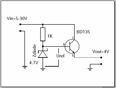
The output voltage of this circuit is Uref - 0.7V. The 0.7V is approximately
the voltage drop between B and E on the transistor. The Z-diode and
the resistor generate a reference voltage which is stable, even if the input
fluctuates and is noisy. The transistor is needed to handle higher currents
than the Z-diode and resistor alone can provide. In this configuration the
transistor just amplifies the current. The current which the resistor and
Z-diode need to provide is the output current divided by hfe (hef is a number
which you can lookup in the datasheet of the transistor).
What are the problems with this circuit?
- The transistor will die when there is a short circuit on the output.
- It provides only a fixed output voltage.
These are quite severe limitations which make this circuit unusable but this
circuit is
still the basic building block of all electronically regulated power supplies.
To overcome those problems you need
some "intelligence" which will regulate the
current on the output and a variable reference voltage. That's all (... and
this makes the circuit much more complex).
For the last few decades people have used operational amplifiers to provide this
intelligence. Operational amplifiers can basically be used as analog calculators to
add, subtract, multiply or logically "or" voltages and currents.
Today microcontrollers are so fast that all this can easily be done in software.
The beauty is that you get as a side effect a voltmeter and an amperemeter
for free. The control loop in the microcontrollers has to know voltage and
current values anyhow. You just need to display it.
What we need from the microcontroller are:
- A AD-converter to measure voltage
and current all the time
- A DA-converter to send commands to our power transistor (provide the
reference voltage)
The problem is that the DA-converter needs to be very fast. If there is a short
circuit detected on the output then we must immediately reduce the voltage
on the basis of the transistor otherwise it will die. Fast means within
milliseconds (as fast as an operational amplifier).
The ATmega8 has an AD-converter which is more than fast enough but it has
at first glance no DA-converter. It is possible to use pulse width modulation
and an analog low pass filter to get an DA-converter but this is much too slow
to implement the short circuit protection in software. How to build a fast
DA-converter?
The R-2R ladder
There are many ways to build a digital to analog converter but we need a
fast and cheap one which can easily interface to our microcontroller.
There is a DA-converter circuit known as "R-2R ladder". It consists of resistors
and switches only. There are two types of resistors. One with R and one
with twice the value of R.
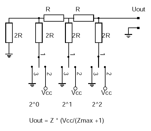
The above shows a 3 bit R2R-DA-converter. The control logic moves the switches
between GND and Vcc. A digital "one" connects the switch to Vcc and a digital
"zero"
to GND. What does this circuit do? It provides voltages in steps of Vcc/8.
In general the output voltage is Z * (Vcc/(Zmax+1) where Z is the digital
number. In the case of a 3 bit AD converter this is: 0-7.
The inner resistance of the circuit as seen from the output is R.
Instead of using separate switches we can connect the R-2R ladder to the
microcontroller output lines. A output pin of the ATmega8 can provide
about 10mA but at this current you will notice already a voltage drop. We would
like to use the full output range from 0-5V in other words the load on the output should
be less than 1mA. We build a R-2R ladder with 5K and 10K
resistors.
The AD-converter of the ATmega8 has a resolution of 10bit. To use the resolution
completely we need also 10bit for the DA-converter.
For this we need 10 output pins which are not used by anything else. This is a little
challenge as we would also like to have a keyboard, LCD display and an I2C serial
interface to the PC. The ATmega8 is quite good. It just fits.
A more detailed design
So here is now a more detailed design of the above circuit.
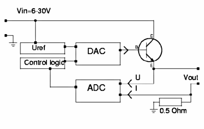
I don't want to
disappoint you but it is unfortunately still a circuit which will not be usable.
However it very good to understand the idea which is behind the real circuit.
So what is wrong with this circuit? There are mainly two things:
- The DAC (digital to analog converter) can not provide the current to drive
the power transistor
- The microcontroller operates at 5V so the maximum output of the DAC is 5V
which means that the maximum output voltage behind the power transistor will be
5-0.7=4.3V .
To fix this we must add amplifiers for current and voltage.
Adding an amplifer stage to the DAC
When adding amplifiers we must keep in mind that those must work with large
signals. Most amplifier designs (e.g for audio) are done under the assumption
that the signals will be small compared to the supply voltage. So forget all the
classic books about transistor amplifier design.
We could use operational amplifiers but those would require extra positive and
negative supply voltages which we want to avoid.
There is also the additional requirement that the amplifier must go from zero
voltage to a stable state without generating any output peek. In other
words there must not be any short oscillation or output peek when you switch
on the power supply.
What to do? Well this is not an easy task at all and requires some experience.
Have a look at the picture below. It shows an amplifier stage which is
suitable for this purpose.
We start with the power transistor. We use a BD245 (Q1). According to the datasheet
this transistor has
a hfe=20 at 3A output. It will therefore draw about 150mA on the basis.
To amplify the current we use
a configuration known as "Darlington transistor". For this we put a medium power
transistor
in front. Those have typically a hfe value of 50-100. This will reduce the current needed to
less than 3mA (150mA / 50).
3mA are manageable with small signal transistors like BC547/BC557. Those
small signal transistors are then very good for building a voltage amplifier.
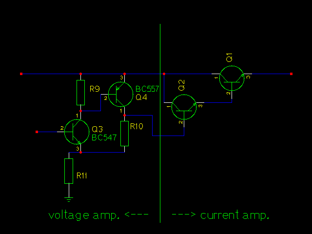
For 30V output we must at least amplify the 5V from the DAC by a factor of 6.
For this we combine a PNP and an NPN transistor as shown below. The voltage amplification
factor of this circuit is:
Vampl= (R10 + R11)/R11
The power supply shall be
available in 2 version: Max 30 output and max 22V output. A combination of 1K
and 6.8K gives a factor of 7.8 which is good for the 30V version and has some
room for possible losses due to higher currents (our formula is linear. The reality
is non-linear). For the 22V
version we use 1K and 4.7K.
The inner resistance of the circuit as seen on the Basis of BC547 is:
Rin=hfe1 * S1 * R11 * R9 = 100 * 50 * 1K * 47K = 235 MOhm

- hfe is about 100 to 200 for a BC547 transistor
- S is the slope of the amplification curve of a transistor and is
 about 50 [unit=1/Ohm]
This is more than high enough for the connection to our DAC which has a inner resistance of 5K.
The inner equivalent output resistance is:
Rout= (R10 + R11) / (S1 + S2 * R9 * R11) = about 2 Ohm
Low enough to drive the following transistor Q2.
R9 ties the basis of BC557 to
the emitter which means "off" for the transistor until the DAC and BC547 come up.
R11 and R10 tie the Basis of Q2 initially to ground which shuts the output
darlington stage down.
In other words every component in this amplifier stage is initially off.
This means we will not get from those transistors any oscillations or output
peeks at power on or power off. A very important point. I have seen expensive
industrial power supplies which produced a voltage peek at power off. Such a
power supply is definitly to be avoided as it can easily kill sensitive
circuits.
The limits
>From previous experience I know that most readers would like to
"customize" the circuit a bit. Here is a list of hardware limits
and how to overcome them:
BD245B: 10A 80W. The 80W are however at a temperature of 25'C
        In other words add a safety margin and calculate with 60W-70W:
        (Max input voltage * Max current) < 65W

        You can add a second BD245B to go up to 120W. To ensure
        that the current distributes equally add a 0.22 Ohm resistor
        into the Emitter line of each BD245B.
        The same circuit and board can be used. Mount the transistors
        on a proper aluminum cooler and connect them with short
        wires to the board. The amplifer can drive a second power transitor
        (that's the maximum) but you might need to adjust the
        amplification factor.

Current measurement shunt:
        We use a 0.5 Ohm resistor with 6W. This is good enough
        for about 3A of output (Iout^2 * 0.50 <= 6W). Use a resistor
        with more watts for higher currents.
Power sources
You can either use a transformer, rectifier and big capacitors or
you can try to get a 32/24V laptop power supply.
I went for the later option. Those laptop power supply "bricks" are
sometimes sold very cheap (over stock) and some of them provide
70W at 24V or even 32V DC.
Most people will probably go for a transformer because those are
very easy to get.
22V 2.5A version:  you need a 18V 3A transformer, a rectifier
                   and a 2200uF or 3300uF capacitor. (reason: 18 * 1.4 = 25V)

30V 2A version:    you need a 24V 2.5A transformer, a rectifier and
                   a 2200uF or 3300uF  capacitor. (reason: 24 * 1.4 = 33.6V)

It does not harm to buy a transformer which can provide more ampere.

A power diodes bridge with 4 diodes which are specified for a
low volatage drop (e.g BYV29-500) gives a good
rectifier.
You can also
use a "heavier" transformer.
Check your circuit for proper insulation. Make sure that it is not possible to
touch any part that may carry 110V/230V even when the case is open.
Connect all metal parts of the chassis to earth (not to GND of the circuit).
Other voltages and current limits
The two provided configurations are 22V 2.5A and 30V 2A. If you want
to build a version with other (lower) output voltages or current limits
then just edit the hardware_settings.h file.
Example: To build a 18V 2.5A version you just edit the hardware_settings.h
file and change the maximum output voltage to 18V.
You can then use a 20V 2.5A power source.
Example: To build a 18V 1.5A version you just edit the hardware_settings.h
file and change the maximum output voltage to 18V and the max. current to
1.5A.
You can then use a 20V 1.5A power source.
Testing
The last component to solder to the board should be the microcontroller.
Before you insert it I would recommend to do some basic hardware tests:
Test1:
Connect some power supply (at least 10V) to the power input of the circuit and
check that you get 5V DC behind the voltage regulator.
Test2: Measure the output voltage. It should be 0V (or near zero, e.g 0.15V, and
it will go to zero if you put a "load" of 2K to 5K on the output.)
Test3: Connect pin 7 and pin 26 on the microcontroller with a wire (solder
a temporary wire connection which you remove before you add later on the
microcontroller on the board). You should get on the output a couple of
volts less than what is used at DC input. Remove the wire and the output
should go back to zero. Be sure to not cause any short circuit on the output.
Solder the microcontroller to the board and load the LCD test software by running the
commands in the directory of the unpacked digitaldcpower tar.gz package.
make test_lcd.hex
make load_test_lcd
You should see "ok works" on the display.
Now you can load the final software as described above.
A word of warning for further testing with the final software: Be careful with short
circuits until you have tested the current limitation function. A save way to
test the current limitation is to use a low Ohm resistor, e.g a car bulb.
Set a low current limit, e.g 30mA at 10V. You should see the voltage
go down immediately
to almost zero once you connect the bulb on the output. There is still a fault
in the circuit if it does not go down. The car bulb will protect the power
supply circuit even if there is a fault as it is not a full short circuit.
The software
This section will give you insights as to how the software
works and you can use the knowledge to do modifications.
However be aware that the short circuit protection is also only
software. If you make a mistake somewhere then this protection
may not work. If you then cause a short circuit on the output
your hardware may go off in a cloud of smoke. To avoid this
you should use a 12V car bulb (see above) to test the short circuit
protection.
Now a bit about the software structure.
First look at the main program (file main.c, download at the end of this
article) you will see
that there are only a few lines of initialization code executed
at power on and then the software enters an endless loop.
There are really 2 endless loops in this software.
One is the main loop ("while(1){ ...}" in file main.c) and the
other one is the periodic interrupt from the Analog the Digital
Converter (function "ISR(ADC_vect){...}" in file analog.c).
During initialization the interrupt is configured to execute every
100μ Sec. All functions and code that is executed runs in
the context of one of those tasks (task the name for a process
or thread of execution in a real time OS, so I use this word here even if
there is no OS).
![[priorities]](../../common/images2/article07071/tasks.gif)
The interrupt task can stop the execution of the main loop at
any time. It will then execute without being interrupted and
then execution continues again in the main loop at the place
where it was interrupted. This has two consequences:
- The code in the interrupt must not be too long as it must
finish before the next interrupt comes. What counts here are
the amount of instructions in machine code. A mathematical
formula, which can be written as just one line of C-code may
result in hundreds of lines of machine code.
- Variables that you share between interrupt code and code
in the main task may suddenly change in the middle of
execution. This is also valid when you hand more than one
byte of data from the interrupt to the main task. The copying of two
bytes will require more than one instruction and then it can
happen that the first byte is copied before the interrupt
while the second byte is copied after the interrupt. What to
do? In most cases it is not a problem because the measurement
results from the ADC will not differ too much between two
interrupts. In cases where you can not afford this type of
occasional fault (it may happen only once every hour) you
have to use a flag which you can check to see if your code
was interrupted during the copying.
All this means that complex things like updating of the
display, checking of push buttons, conversion of ampere and
volt values to internal units etc ... must be done in the main
task. In the interrupt we execute only things that are time
critical: Current and voltage control, overload protection and
setting of the DAC. To avoid complex mathematics all
calculations in the interrupt are done in ADC units. That is
the same units that the ADC produces (integer values from
0...1023).
Here is the exact logical flow of operations that we do in the
main task:
1) Copy the latest ADC results from the interrupt task
2) Convert them into display values (ampere and volt)
3) Convert the wanted ampere and volt values (what the user has set)
   to internal equivalent ADC values
4) Copy the wanted equivalent ADC values to variables such that
   the interrupt task can use them.
5) Clear the LCD display
6) Convert the numbers which we want to display on the LCD into
   strings.
7) Write voltage values to the display.
8) Check if the interrupt task regulates currently voltage or current
   (current limitation active)
9) If voltage is the limiting factor then write an arrow behind
   voltage on the display
10) Write ampere values to the display
11) Check if the interrupt task regulates currently voltage or current
    (current limitation active)
12) If current is the limiting factor then write an arrow behind
    current on the display
13) Check if a button was pressed. If not wait 100ms and check again.
    If a button was pressed then wait 200ms. This is to have a good
    response of the buttons and not too fast scrolling if they are
    permanently pressed.
14) Go to step 1).
The interrupt task is much simpler:
1) Copy the results from the ADC to variables
2) Toggle the ADC measurement channel between current and voltage
3) Check if excessive current is measured. If so set the DAC immediately
   to a low value (It does not have to be zero since the voltage
   amplifier circuit works only from 0.6V on (0.6 volt input
   produce still 0 volt output)).
4) Check if voltage or current needs to be regulated
5) Check if the DAC (digital to analog converter) needs updating
   according to the decision from 4).
This is the basic idea of the software. I will also explain
what you find in which files and then you should be able to
understand the code (given that you are familiar with C).
Software: Which file contains what
main.c -- this file contains the main program. All initialization is
         done from here.here.  The main loop is also implemented here.

analog.c -- the analog to digital converter and everything that
         runs in the context of the interrupt task can be found here.

dac.c -- the digital to analog converter. Initialized from ddcp.c but
         used only from analog.c

kbd.c -- the keyboard code

lcd.c -- the LCD driver. This is a special version which will not need
         the rw pin of the display. It uses instead an internal timer
         which should be long enough for the display to finish its task.
Loading and using the software
Now you want to know how the use the software and how to load
it.
Unpack the digitaldcpower tar.gz package and "cd" into the directory
that is created.
Edit the file hardware_settings.h and adjust it according to the hardware.
Here you can also do calibrations of voltmeter and amperemeter. The file
is well commented.
gedit hardware_settings.h
Connect the programmer cable and power on the circuit.
Then run:
make wrfuse4mhz

This will set the clock frequency of the microcontroller to 4MHz. The
software is designed for this frequency.

make

This will compile the software.

make load

This will load the software.
Control of the power supply unit from any PC (Win, Linux, Mac,...)
This lab/bench power supply can be controlled not only locally from the front
pannel but also via command.
That is: You can optionally connect a computer and give a command to say "produce 6V"
and the power supply will change to 6V. A really cool feature for automated
testing.
To remotely control the power supply via commands we will use
again I2C communication (see also A simple digital thermometer). I2C communication is a bit
slow but we do not send long commands. A command to set the
voltage could e.g be as short as "u=12". This is still human
readable and understandable but only a few bytes long.
The software to do this remote control has by now been ported
to Linux, Windows, Mac OS X and Solaris. It is probably
quite easy to port this code to even more operating systems.
How control via I2C works
I2C is a protocol over a two wire bus. One line on the bus
carries the clock (SCL) and the other the data (SDA). This has the big
advantage that you do not need a precise synchronous clock
signal. The timing is not so important for I2C therefore it is very
easy to implement in a simple user space program (no special
kernel module). For the physical interface we use again the
rs232 modem control lines. USB is also possible to use via a
USB to serial converter. The new Apple Macs have e.g no rs232
but because I2C is not sensitive to timing it is
possible to use adapter cables such as the Prolific PL-2303
(there are some links to USB adapters in the software for this
article under other_OS/macOSX/README.txt, see download at the
end of this article).
The program to send commands to our DC power supply is a
simple command line based program called i2ctalk. It is
available in source code and as precompiled binary for Linux, Solaris,
Mac OSX and Windows. You use it like this:
I2C commands for the DC power supply:
=====================================

# set Imax to 0.20A:
i2ctalk i=20
# get current I value:
i2ctalk i
# store current settings
i2ctalk s
# set Umax to 2.1V:
i2ctalk u=21
# get current voltage value:
i2ctalk u
You can enhance the program and build a fancy graphical
application if you want. I have just tired to keep it as simple
as possible.
The buttons
The power supply has 4 button for local control of voltage and max. current.
The 5-th button is to store the settings permanently in an eeprom such that
it will come on with identical settings the next time you power it on.
![[buttons]](../../common/images2/article07071/buttons.gif)
The local control button pad.
With U+ you can increase the voltage and with U- you decrease it. When you
hold the button then it will step and after a while "run" faster to make
it easy to change the voltage in large steps. The I+ and I- buttons work
the same way.
The display
This is how the display looks like:
![[display]](../../common/images2/article07071/display.png)
The fields in the LCD display area. The real measured
values and the set values are always shown at the same time.
The arrow on the right indicates that currently the configured voltage
is the limiting factor. Should a short circuit occur on the output or
the connected device draws more current then the arrow will flip to the
bottom line and indicate that the configured max. current has become the limiting
factor.
Blocking HF interference
DC-motors without filters and other devices containing large coils
can generate strong high frequency signals. Those can potentially
interfere with the LCD display electronics.
The result can be funny characters on the display.
The microcontroller itself is not so sensitive as it is mostly self contained.
The interference depends also to a large degree on how the internal wiring inside
the case of the power supply is done. Longer cables between display and
circuit board act as antennas which can easily pick-up HF signals. In any case
the best solution is to block HF signals directly at the front connector
of the power supply.
Solder a ceramic capacitor in the range of 10nF to 100nF directly
behind front connectors:
![[block HF signals]](../../common/images2/article07071/ddcp9.jpg)
A ceramic capacitor between the power output connectors to
block HF-signals from coming into the power supply.
Some pictures and ideas
Here are some pictures from the power supply(s) which I have build.
Pictures are sometimes much better than long description especially when
it comes to hardware and mechanical parts.

You can build a simple but professionally looking case from an
aluminum sheet and two wooden boards.

Just bend the aluminum twice. This is easy to do even without
professional equipment.
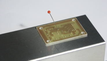
Mark the positions of the push buttons on the case before you
solder the buttons onto the board. This makes it easy to drill the
holes at the right position.
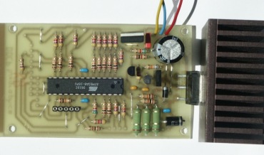
The circuit. Very small but with more features and more powerful than many
other power supply circuits.
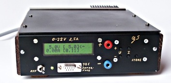
The final power supply unit. With a green display.
... and with a blue display. It looks cool and is very small. Just 4.5cm high. Incredible
what such a small power supply can do. Blue displays are bit difficult to
photograph.
It looks even better in reality than here on the photo.
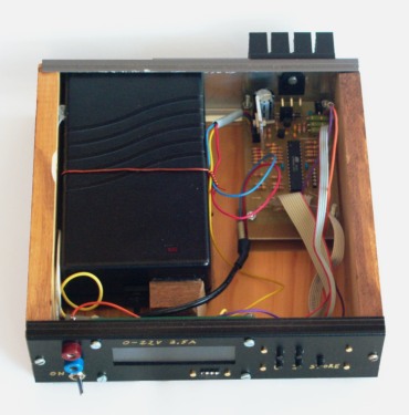
How it looks inside. I used an old 24V 3A laptop power supply "brick"
as power source. They are very compact and don't need additional rectifiers
or capacitors.
|
Have fun! I am sure you will like this power supply unit. I use it a lot
and every day.
References/Download
- Download page for this article
(firmware updates and corrections will also be available from here).
- Datasheet for the ATmega8: go to http://www.atmel.com/
and select products->Microcontrollers ->AVR-8 bit
RISC->Documentation->datasheets
- Tuxgraphics electronics section, a collection of all articles in this series.
- Tuxgraphics
online shop, You can order this power supply unit as a kit from here.
The kit includes not only the parts but also additional documentation
and the circuit diagram.
© Guido Socher, tuxgraphics.org
2008-05-18, generated by tuxgrparser version 2.55